- 您现在的位置:买卖IC网 > Sheet目录493 > NVB25P06T4G (ON Semiconductor)MOSFET P-CH 60V 27.5A D2PAK
�� �
�
�NTB25P06,� NVB25P06�
�Power� MOSFET�
�?� 60� V,� ?� 27.5� A,� P� ?� Channel� D� 2� PAK�
�Designed� for� low� voltage,� high� speed� switching� applications� and� to�
�withstand� high� energy� in� the� avalanche� and� commutation� modes.�
�Features�
�?� AEC� Q101� Qualified� ?� NVB25P06�
�?� These� Devices� are� Pb� ?� Free� and� are� RoHS� Compliant�
�Typical� Applications�
�?� PWM� Motor� Controls�
�?� Power� Supplies�
�?� Converters�
�?� Bridge� Circuits�
�V� (BR)DSS�
�?� 60� V�
�http://onsemi.com�
�R� DS(on)� TYP�
�65� m� W� @� ?� 10� V�
�P� ?� Channel�
�D�
�I� D� MAX�
�?� 27.5� A�
�MAXIMUM� RATINGS� (T� J� =� 25� °� C� unless� otherwise� noted)�
�Rating� Symbol�
�Value�
�Unit�
�G�
�Drain� ?� to� ?� Source� Voltage�
�Gate� ?� to� ?� Source� Voltage�
�?� Continuous�
�?� Non� ?� Repetitive� (t� p� v� 10� ms)�
�V� DSS�
�V� GS�
�V� GSM�
�?� 60�
�"� 15�
�"� 20�
�V�
�V�
�Vpk�
�S�
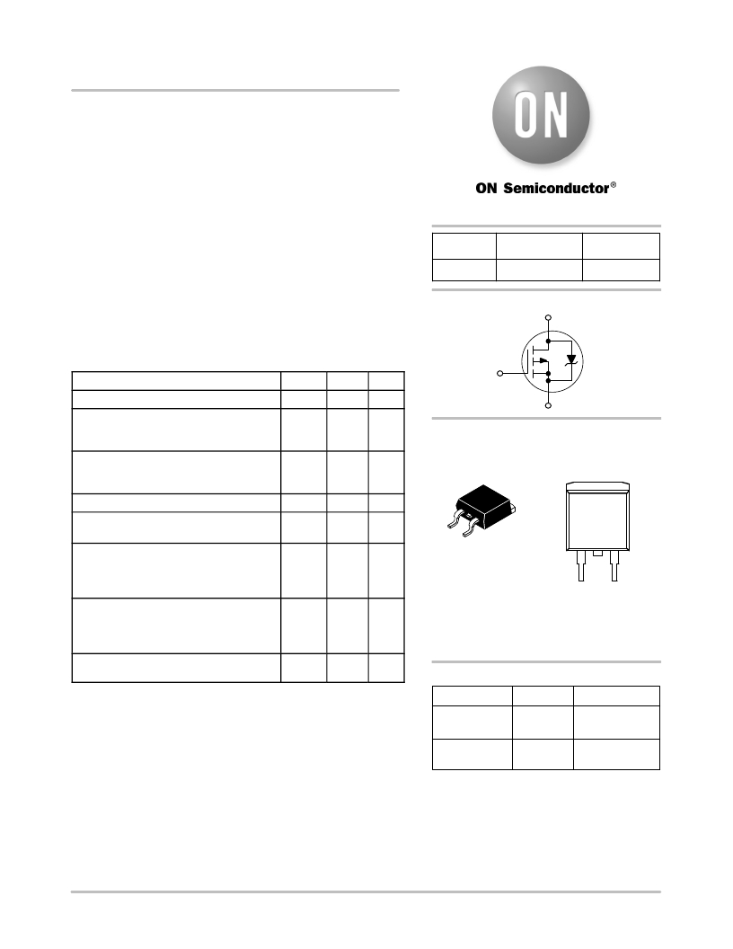
�MARKING� DIAGRAM�
�&� PIN� ASSIGNMENT�
�Drain� Current�
�?� Continuous� @� T� A� =� 25� °� C�
�?� Single� Pulse� (t� p� v� 10� m� s)�
�I� D�
�I� DM�
�27.5�
�80�
�A�
�Apk�
�Drain�
�Total� Power� Dissipation� @� T� A� =� 25� °� C�
�Operating� and� Storage�
�Temperature� Range�
�Single� Pulse� Drain� ?� to� ?� Source� Avalanche�
�Energy� ?� Starting� T� J� =� 25� °� C�
�(V� DD� =� 25� V,� V� GS� =� 10� V,�
�I� L(pk)� =� 20� A,� L� =� 3� mH,� R� G� =� 25� W� )�
�P� D�
�T� J� ,� T� stg�
�E� AS�
�120�
�?� 55� to�
�+175�
�600�
�W�
�°� C�
�mJ�
�1�
�2�
�3�
�D� 2� PAK�
�CASE� 418B�
�4�
�Gate�
�NTB�
�25P06G�
�AYWW�
�Drain�
�Source�
�Thermal� Resistance�
�?� Junction� ?� to� ?� Case�
�?� Junction� ?� to� ?� Ambient� (Note� 1)�
�?� Junction� ?� to� ?� Ambient� (Note� 2)�
�R� q� JC�
�R� q� JA�
�R� q� JA�
�1.25�
�46.8�
�63.2�
�°� C/W�
�A�
�Y�
�WW�
�G�
�=� Assembly� Location�
�=� Year�
�=� Work� Week�
�=� Pb� ?� Free� Package�
�Maximum� Lead� Temperature� for� Soldering�
�Purposes,� (1/8� ″� from� case� for� 10� s)�
�T� L�
�260�
�°� C�
�ORDERING� INFORMATION�
�Stresses� exceeding� Maximum� Ratings� may� damage� the� device.� Maximum�
�Ratings� are� stress� ratings� only.� Functional� operation� above� the� Recommended�
�Operating� Conditions� is� not� implied.� Extended� exposure� to� stresses� above� the�
�Recommended� Operating� Conditions� may� affect� device� reliability.�
�1.� When� surface� mounted� to� an� FR4� board� using� 1� ″� pad� size�
�(Cu� Area� 1.127� in� 2� ).�
�2.� When� surface� mounted� to� an� FR4� board� using� the� minimum� recommended�
�pad� size� (Cu� Area� 0.412� in� 2� ).�
�Device�
�NTB25P06T4G�
�NVB25P06T4G�
�Package�
�D� 2� PAK�
�(Pb� ?� Free)�
�D� 2� PAK�
�(Pb� ?� Free)�
�Shipping� ?�
�800� /� Tape� &� Reel�
�800� /� Tape� &� Reel�
�?For� information� on� tape� and� reel� specifications,�
�including� part� orientation� and� tape� sizes,� please�
�refer� to� our� Tape� and� Reel� Packaging� Specification�
�Brochure,� BRD8011/D.�
�?� Semiconductor� Components� Industries,� LLC,� 2011�
�October,� 2011� ?� Rev.� 4�
�1�
�Publication� Order� Number:�
�NTB25P06/D�
�发布紧急采购,3分钟左右您将得到回复。
相关PDF资料
NVB6410ANT4G
MSOFET N-CH 100V 76A D2PAK
NVD4815NT4G
MOSFET N-CH 30V 6.9A DPAK-4
NVD5117PLT4G
MOSFET P-CH 60V 61A DPAK
NVD5803NT4G
MOSFET N-CH 40V 85A DPAK
NVD5807NT4G
MOSFET N-CH 40V 23A DPAK
NVD5862NT4G
MOSFET N-CH 60V 90A DPAK-4
NVD5863NLT4G
MOSFET N-CH 60V 14.9A DPAK-4
NVD5865NLT4G
MOSFET N CH 60V DPAK-4
相关代理商/技术参数
NVB-2B
制造商:NUMATIC 功能描述:VACUUM CLEANER HOSES
NVB300
制造商:Aavid Thermalloy 功能描述:HEAT SINK ((NS))
NVB5404NT4G
功能描述:MOSFET NFET D2PK 40V 129A 4.5MOH RoHS:否 制造商:STMicroelectronics 晶体管极性:N-Channel 汲极/源极击穿电压:650 V 闸/源击穿电压:25 V 漏极连续电流:130 A 电阻汲极/源极 RDS(导通):0.014 Ohms 配置:Single 最大工作温度: 安装风格:Through Hole 封装 / 箱体:Max247 封装:Tube
NVB5405NT4G
功能描述:MOSFET AUTOMOTIVE MOSFET
RoHS:否 制造商:STMicroelectronics 晶体管极性:N-Channel 汲极/源极击穿电压:650 V 闸/源击穿电压:25 V 漏极连续电流:130 A 电阻汲极/源极 RDS(导通):0.014 Ohms 配置:Single 最大工作温度: 安装风格:Through Hole 封装 / 箱体:Max247 封装:Tube
NVB5426N
制造商:ONSEMI 制造商全称:ON Semiconductor 功能描述:Power MOSFET 120 Amps, 60 Volts N-Channel D2PAK, TO-220
NVB5426NT4G
功能描述:MOSFET AUTOMOTIVE MOSFET
RoHS:否 制造商:STMicroelectronics 晶体管极性:N-Channel 汲极/源极击穿电压:650 V 闸/源击穿电压:25 V 漏极连续电流:130 A 电阻汲极/源极 RDS(导通):0.014 Ohms 配置:Single 最大工作温度: 安装风格:Through Hole 封装 / 箱体:Max247 封装:Tube
NVB5860N
制造商:ONSEMI 制造商全称:ON Semiconductor 功能描述:N-Channel Power MOSFET
NVB5860NL
制造商:ONSEMI 制造商全称:ON Semiconductor 功能描述:N-Channel Power MOSFET